|
|||||
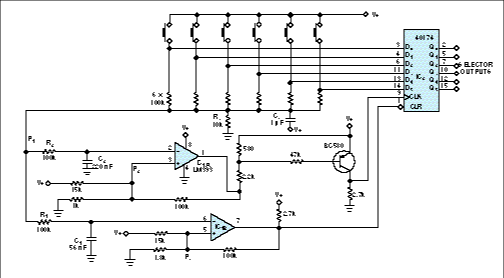
June 5, 1997 Debouncing networks make reliable selectorW Dijkstra, Waalre, The Netherlands The expandable selector in Figure 1 consists of six switches, a HEX D-type flip-flop and two comparators with hysteresis and debouncing networks. The debouncing networks ensure that only one output of IC2 is high at any time, and you can expand this circuit using more switches and D-type flip-flops. All outputs of IC2 are low after power-on because the R3-C3 network delivers a short, low-level pulse at the clear input of IC2. The trigger point of comparator IC1A at P2 is approximately 0.07×V+, and the trigger point of comparator IC1B at P3 is approximately 0.12×V+. When you push one switch, the magnitude of the voltage at P1 is 0.09×V+, so only the output of IC1A goes low, producing a positive pulse at IC2's clock input. In this case, only one D input is high, so after the clock pulses, only one output is high. When you simultaneously push two or more switches, the magnitude of the voltage at P1 is at least 0. 17×V+, so both comparator outputs go low. However, the output of IC1B goes low before IC1A's output because the R1-C1 debouncing network's time-constant is shorter than the R2-C2 network's time-constant. The resulting low level at the clear input of IC2 causes all outputs to go low. Thus, it is impossible that more than one output of IC2 is high. (DI #2028) |
|||||
|
|||||
| EDN Access | Feedback | Table of Contents | |
|||||
| Copyright © 1997 EDN Magazine, EDN Access. EDN is a registered trademark of Reed Properties Inc, used under license. EDN is published by Cahners Publishing Company, a unit of Reed Elsevier Inc. | |||||